
Nvidia to accelerate chip manufacturing processes using AI and digital twins
Nvidia introduces the AI-defined fab concept, leveraging AI, digital twins, and physics-based machine learning to accelerate chip manufacturing.
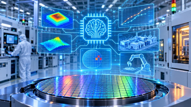
Behind the production of mass semiconductor products lies a massive layer of engineering work. During process and chip design phases, R&D employees make decisions that later affect both chip performance and defect rates. Artificial intelligence provides an opportunity to reduce engineering errors and consider more successful options with less time expenditure.
- The AI-defined fab concept integrates artificial intelligence into design, simulation, and quality control.
- Nvidia cuDSS and PhysicsNeMo libraries accelerate physics simulations by up to 35x.
- Lam Research predicts plasma etching behavior in milliseconds instead of days.
- Omniverse-based digital twins allow testing facility changes in a virtual environment.
The AI-defined fab concept and physics simulation acceleration
To assist engineers across all stages of chip implementation and production, Nvidia introduced the AI-defined fab concept, referring to AI-managed semiconductor factories. This does not mean fully autonomous enterprises yet, but rather the integration of artificial intelligence into process design, physical phenomenon simulation, quality control, and production management. Accelerated computing, physics-informed machine learning models, and digital twins allow engineers to test decisions faster.
One key area is accelerating multidisciplinary physics simulations that simultaneously account for heat transfer, electrical processes, and mechanical stress. COMSOL utilizes the Nvidia cuDSS library to accelerate such calculations during semiconductor equipment development with up to a tenfold performance increase. Furthermore, Nvidia's collaboration with Applied Materials covers atomic-level material simulation using platforms like Ginestra powered by cuDSS.
Read alsoNvidia requires cloud partners to allocate 51 percent of services outside ChinaLithography and millisecond-level process predictions
Applied Materials' ACE+ system utilizing PhysicsNeMo speeds up surface topography simulation by up to 35 times. Siemens is integrating the cuLitho library into its Calibre software, achieving up to 17x acceleration in specific computational tasks. Another approach involves using AI models trained on physics simulation results to predict process behavior without rerunning full computational simulations.
A prime example is Lam Research applying Nvidia PhysicsNeMo to predict the behavior of plasma used in silicon wafer etching. Such calculations require accounting for electrical, chemical, and thermal processes, and the model can now deliver predictions in milliseconds instead of the days required for physical experiments. This eliminates the need for expensive trial-and-error testing directly on production lines.
Digital twins and manufacturing management agents
AI agents and digital twins complement this ecosystem at the testing and production management levels. Advantest uses Nvidia NeMo Switchyard agents to automatically select appropriate AI models when analyzing semiconductor test results, cutting operation times from hours to minutes. Applied Materials builds digital twins of entire fabrication plants using Nvidia Omniverse libraries.
Together, these advanced processes create the foundation for a new approach to microchip manufacturing where engineers retain control over technological decisions while receiving analysis results much faster. Ultimately, this enables the faster release of higher-quality electronics and computing hardware to the market.
Source: 3DNews: