Siemens and Nvidia team up for AI-powered PCB defect detection
Siemens and Nvidia are developing an AI-driven PCB quality control system that reduces engineering efforts by 85% and false alarms by 40%.
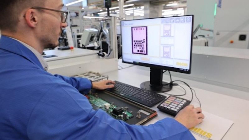
Siemens and Nvidia are joining forces to develop an advanced quality control system for printed circuit boards. The solution allows manufacturers to prepare inspection equipment for defect detection even before the first physical prototype is ever produced.
- The solution integrates Siemens Teamcenter and Process Preparation X with the Nvidia Cosmos platform.
- It uses digital twins and synthetic AI-generated images to pre-calibrate automated optical inspection systems.
- Testing is underway at the Siemens plant in Erlangen to cut manual engineering tasks by 85% and false positives by 40%.
Core Architecture and Digital Twins
At the heart of the new solution are Siemens Teamcenter and Process Preparation X software products, combined with the Nvidia Cosmos platform. Teamcenter provides essential data regarding board design, components, and layout, while Process Preparation X compiles this information into a digital twin.
Based on this digital twin, a virtual golden board is established as a benchmark for the production line. This eliminates the need to manufacture physical test boards ahead of time, significantly speeding up the initial setup phase for new electronics products.
Read alsoDOJ probes Nvidia over Hugging Face acquisition worth 13 billion dollarsNvidia Cosmos and Synthetic Image Generation
Nvidia Cosmos is utilized to generate photorealistic synthetic images of both functional boards and potential manufacturing defects. This synthetic data trains and pre-calibrates Automated Optical Inspection systems using cameras and advanced image analysis algorithms.
The AI-powered system also provides ongoing support once production is officially active. If AOI equipment flags a suspicious area, an additional verification module analyzes whether the issue is a genuine defect or simply a false positive.
Implementation at the Erlangen Factory
The technology is currently being showcased at the Siemens Electronics Factory in Erlangen, Germany. The facility serves as a testing ground for adaptive manufacturing, with Siemens aiming to introduce process changes three to five times a week without halting production.
Project targets indicate a potential reduction in manual engineering effort for optical inspection programs by 85 percent, a 40 percent drop in false alarms, and a greater than 5 percent increase in the yield of boards passing inspection on the first pass.
Impact on Electronics Manufacturing
By unifying optical inspection preparation, calibration, and final verification into a single streamlined workflow, the Siemens and Nvidia collaboration empowers electronics manufacturers to launch new board variants much faster without waiting for physical prototypes.
Source: iXBT.com