Tesla unveils AI accelerator roadmap and shifts to SI branding
Tesla updated its chip roadmap, adopting the Super Intelligence (SI) brand and reviving the Dojo training accelerator project.
Tesla has disclosed its revamped accelerator roadmap, detailing the future of its custom silicon development for autonomous driving and data centers. The company is shifting away from artificial intelligence terminology in favor of super intelligence, rebranding its chips accordingly.
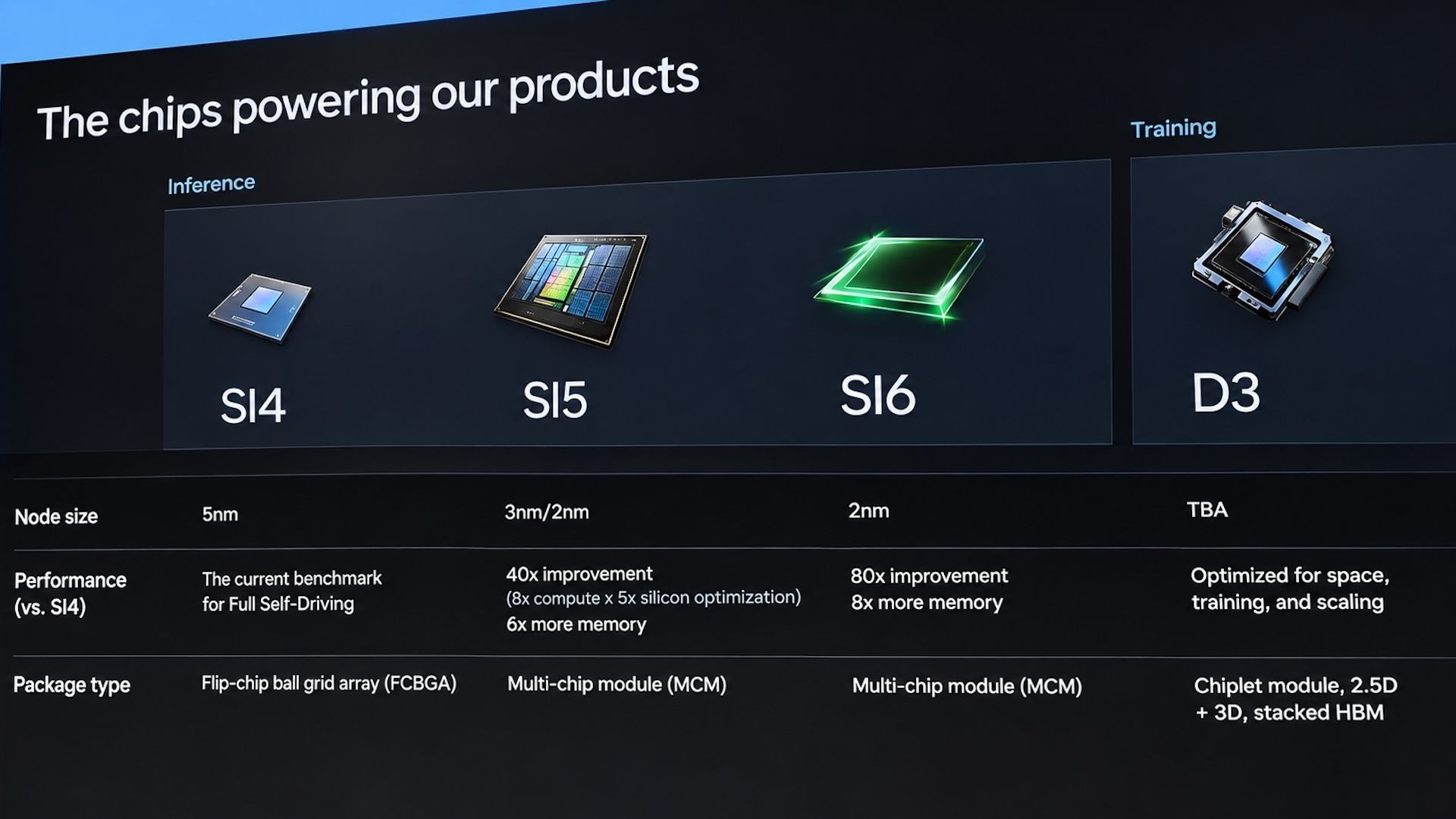
- Tesla renamed its inference accelerators to SI4, SI5, and SI6 instead of using the previous AI monikers.
- The Dojo D3 training accelerator abandons the SRAM wafer-scale design in favor of a multi-chiplet architecture with stacked HBM.
- The 6th generation SI6 inference chip is projected to deliver up to 80 times the compute performance of the 4th generation.
Transition to Super Intelligence Branding
In a recent presentation, Tesla labeled its upcoming processors as SI4, SI5, and SI6, moving away from the previous AI terminology. This update aligns with a broader trend of adopting the super intelligence phrasing, with Elon Musk confirming similar renamings across related ventures.
This rebranding reflects both marketing updates and a serious hardware strategy aimed at delivering immense computational power for future autonomous systems, robotics, and large-scale data processing.
Read alsoTSMC and Samsung shares crash following sell-off across Asian marketsThe Return of Dojo and the D3 Accelerator
Despite previous reports of scaling back the wafer-scale Dojo project, the in-house training accelerator has re-emerged as the Dojo D3. Unlike the first two generations, D3 adopts a chiplet-based design combining 2.5D and 3D packaging with stacked HBM.
The adoption of High Bandwidth Memory addresses the memory capacity constraints of modern AI models. Furthermore, D3 is optimized for space, training, and scaling, suggesting potential deployment in extraterrestrial data centers with radiation-hardened variants.
Specifications of SI5 and SI6 Processors
The upcoming 5th generation inference chip, SI5, will be manufactured using TSMC's 3nm and Samsung's 2nm nodes, delivering a 40X performance improvement over HW4 alongside 96 GB of memory, with power consumption ranging from 250W to 800W.
Looking further ahead, the 6th generation SI6 accelerator slated for 2029-2030 promises an 80X compute improvement and massive memory gains, cementing Tesla's long-term silicon ambitions.
What This Means for the Industry
Tesla's updated roadmap highlights its commitment to vertically integrated hardware. By transitioning to advanced process nodes and HBM memory, the company continues to push the boundaries of automotive and data center computing.
Source: Latest from Tom's Hardware